Intel is at a defining crossroads in the semiconductor industry as it aggressively pushes forward with its most advanced chip technology yet. After years of struggling to keep up with Taiwan Semiconductor Manufacturing Company (TSMC) and Samsung, Intel’s upcoming 18A process node (equivalent to 1.8nm) represents a potential turning point in its fight to regain manufacturing supremacy. The recent successful power-on tests with foundry customers mark a crucial milestone in Intel’s roadmap, but the battle is far from won.
PowerVia: Intel’s Secret Weapon?
One of Intel’s biggest bets in this technological race is PowerVia, its cutting-edge backside power delivery system. This innovation reroutes power delivery to the back of the chip, reducing electrical resistance and improving efficiency. If successful, this will give Intel a competitive advantage, as TSMC is not expected to implement similar technology until at least 2026.
Backside power delivery could be a game-changer, enhancing transistor performance and power efficiency—two critical metrics for data centers, AI workloads, and mobile applications. However, scaling this innovation to high-volume manufacturing remains a formidable challenge. TSMC and Samsung, while behind in this specific technology, have a track record of superior execution in advanced node production.
The Stakes: Intel’s Future Hangs on 18A
Intel CEO Pat Gelsinger has placed the company’s future on the success of its 18A process node, the final phase of Intel’s ambitious “five nodes in four years” strategy launched in 2021. If Intel delivers on this aggressive roadmap, it could signal the company’s resurgence as the world’s leading semiconductor manufacturer. However, execution risks remain high.
Challenges: Manufacturing, Market Share, and AI Shift
While Intel is making bold strides, it faces three major challenges:
- Manufacturing Execution Risks
Intel has historically struggled with manufacturing consistency, as seen in the delays of 10nm and 7nm (now rebranded as Intel 7 and Intel 4). Achieving high yields at 18A will be crucial, especially since foundry customers—including Qualcomm and Amazon AWS—are watching closely before committing to Intel’s manufacturing ecosystem. - Losing Ground to AMD and TSMC
Intel’s server dominance is slipping, with AMD’s EPYC processors (built on TSMC’s cutting-edge nodes) gaining traction in cloud and enterprise markets. For the first time in history, AMD recently surpassed Intel in data center revenue, a sign that hyperscalers (Amazon, Microsoft, Google) are shifting workloads to more efficient alternatives. - AI Disruption and Competitive Pressures
The semiconductor industry is undergoing a massive shift toward AI accelerators, where NVIDIA currently dominates with its H100 and upcoming Blackwell architecture. Intel, while making strides with its Gaudi AI chips, is still playing catch-up. The success of Intel 18A could determine whether the company remains relevant in this rapidly evolving AI-driven landscape.
TSMC and Samsung: The Battle for 2nm and Beyond
Intel is not fighting this battle alone. TSMC plans to start mass production of its 2nm (N2) node in 2025, while Samsung is working on its own 2nm roadmap with GAA (Gate-All-Around) transistors.
TSMC’s 2nm process will introduce nanosheet transistors, a successor to FinFET technology that allows for better performance scaling. Samsung, meanwhile, has already implemented GAA in its 3nm process—a move that, while challenging, could give it a future lead.
Intel’s ability to compete will depend on whether its 18A node arrives ahead of TSMC’s 2nm and whether it delivers real-world performance and efficiency benefits over rival offerings.
Intel’s Foundry Gamble: Can It Take on TSMC?
Beyond its own chips, Intel is betting big on Intel Foundry Services (IFS)—a division created to challenge TSMC’s dominance as a contract chip manufacturer. Intel hopes to attract external customers, but convincing major players like Apple, Qualcomm, and NVIDIA to switch away from TSMC will require flawless execution.
The semiconductor industry is known for long-term customer relationships and trust in supply reliability—two areas where TSMC and Samsung have a major advantage. If Intel fails to meet deadlines or experiences yield issues at 18A, it could struggle to attract foundry customers, making it difficult to justify its $100 billion investment in new U.S. fabrication plants.
A Make-or-Break Moment for Intel
The next 18 months will determine whether Intel can reclaim its chipmaking crown or fall further behind in the industry. 18A could be the company’s comeback story—or its biggest misstep yet.
With TSMC and Samsung racing toward 2nm and AI reshaping the semiconductor landscape, Intel must not only deliver on its promises but do so at a level that regains customer trust and reestablishes its reputation as the undisputed leader in advanced semiconductor manufacturing.
Key Takeaways
- Intel’s 18A node has passed crucial testing phases and remains on track for 2025 production
- New PowerVia technology promises significant performance gains over current manufacturing methods
- Intel’s manufacturing comeback strategy centers on delivering five process nodes within four years
Revolutionizing Chip Architecture and Performance
Intel’s latest technological advancements mark a significant shift in semiconductor manufacturing, with new transistor designs and power delivery systems that aim to improve performance and efficiency across their product lineup.
Innovations in Transistor Design and Process Technology
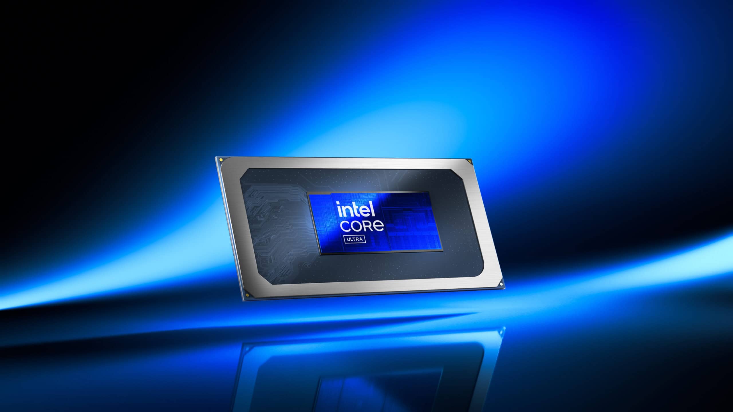
Intel’s 18A process node represents a significant advancement in chip manufacturing. The company has replaced traditional FinFET transistors with ribbonFET architecture, a gate-all-around design that increases current flow and reduces power leakage.
The revolutionary PowerVia technology implements backside power delivery, separating the power delivery network from the signal network. This design reduces signal loss and improves overall chip efficiency.
Key improvements in the 18A process include:
- 25% higher transistor density
- 18% performance gain per watt
- Reduced power consumption
- Enhanced signal integrity
Intel’s Next-Generation Products
Panther Lake CPUs will launch in late 2025, built on the 18A process node. These processors will integrate AI acceleration capabilities and enhanced efficiency cores.
The product roadmap includes:
- Meteor Lake: First disaggregated design
- Granite Rapids: Server-focused architecture
- Panther Lake: Next-gen consumer platform
Scaling for Efficiency and Power
The new process node implements advanced EUV lithography for precise pattern creation at smaller scales. This enables higher transistor density while maintaining power efficiency.
PowerVia technology creates dedicated layers for power delivery, reducing signal interference and improving performance. The separation of power and signal layers allows for:
- Optimized power distribution
- Reduced signal noise
- Better thermal management
- Improved voltage control
These innovations enable Intel to scale chip designs more effectively while maintaining reasonable power consumption levels.
Strategic Movements and Industry Impact
Intel has committed to investing more than $100 billion over five years in new chipmaking capabilities, aiming to reclaim its position as the industry leader in semiconductor manufacturing.
Intel’s Competitive Position and Collaborations
Intel CEO Pat Gelsinger has implemented the IDM 2.0 strategy to transform the company’s manufacturing capabilities and market position. This strategy opens Intel’s foundry services to external customers, competing directly with TSMC and Samsung.
The company has established partnerships with key industry players like ASML to secure advanced lithography equipment. These collaborations strengthen Intel’s ability to produce cutting-edge chips.
Intel faces strong competition from TSMC, which currently leads in advanced node manufacturing. TSMC’s 2nm process commands premium pricing at $30,000 per wafer, creating opportunities for Intel to offer competitive alternatives.
Intel’s Manufacturing and Technological Advancements
Intel’s 18A process node features innovative PowerVia technology for backside power delivery. This advancement gives Intel a significant advantage, as TSMC won’t implement similar technology until 2026.
The company has made substantial progress in 3D advanced packaging technologies, including Foveros Omni and Foveros Direct. These technologies enable more efficient chip designs and better performance.
Intel’s manufacturing roadmap aims to match TSMC’s capabilities by 2024. The company is working to overcome past challenges, such as delays in 10nm production.
The Future of Semiconductor Manufacturing
The semiconductor industry is entering the Angstrom era of chip manufacturing, with Intel leading development of sub-2nm processes. This advancement promises significant improvements in power efficiency and performance.
An overreliance on a single manufacturer could create monopolistic conditions. The industry benefits from competition between Intel, TSMC, and Samsung.
Advanced packaging technologies and through-silicon vias will play crucial roles in future chip designs. These innovations enable more complex integrated circuits and improved performance scaling.