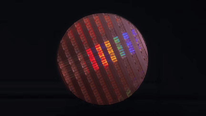
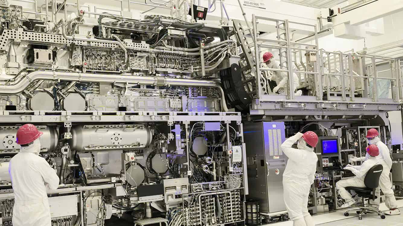
Intel’s 18A process node represents a significant leap forward in semiconductor manufacturing technology. Intel plans to begin production of 18A-based chips in 2025, marking a major milestone in the company’s roadmap for advanced chip fabrication. This cutting-edge process promises to deliver substantial improvements in performance and efficiency for future processors.
The 18A node incorporates innovative features like RibbonFET and PowerVia technologies. These advancements aim to enhance transistor performance and power delivery in next-generation chips. Intel has already achieved key milestones, with 18A-based products successfully powering on and booting operating systems.
Intel’s progress with 18A has implications beyond its own product lines. The company plans to offer 18A manufacturing capabilities to external customers through its Intel Foundry Services division. This move positions Intel to compete more directly with other leading semiconductor foundries in the race to produce cutting-edge chips.
Understanding Intel’s 18A Process

What is Intel 18A?
Intel 18A is Intel’s next major step in chip manufacturing. It uses new technologies to make smaller, faster, and more energy-efficient chips. Two key features define 18A:
- RibbonFET: This is a new type of transistor, like a tiny switch that controls the flow of electricity in a chip. It lets more current flow through the transistor when it’s on, and less when it’s off, making the chip faster and use less power.
- PowerVia: This puts the power connections on the back of the chip. This frees up space on the front for more transistors, making the chip smaller and more powerful. It also improves power delivery, which makes the chip more efficient.
What are the Benefits of 18A?
These new technologies offer several advantages:
- Improved Performance: More transistors and better power delivery mean faster processing speeds.
- Lower Power Consumption: More efficient transistors and power delivery lead to less wasted energy.
- Smaller Chip Size: Putting power connections on the back lets Intel pack more transistors into a smaller space.
What Products Will Use 18A?
Intel plans to use 18A in various products:
- Panther Lake CPUs: These are processors for desktop and laptop computers. They should be available in 2025.
- Clearwater Forest CPUs: These are processors for servers and data centers. They will offer high performance for demanding tasks.
How Does 18A Compare to Other Technologies?
Intel 18A aims to compete with the most advanced chip manufacturing processes from other companies like TSMC and Samsung. TSMC’s N2 (2nm-class) node is also on the horizon. Here’s a comparison:
| Feature | Intel 18A | TSMC N2 |
|---|---|---|
| Key Transistor Tech | RibbonFET (Gate-All-Around) | FinFET (Likely transitioning to Gate-All-Around) |
| Power Delivery | PowerVia (Backside Power) | Frontside power delivery (Likely transitioning to Backside Power) |
| Expected Availability | 2025 (Initial Production), 2026 (High-Volume Manufacturing) | 2025 (Expected) |
It is important to note that the exact performance and power efficiency of each process will depend on the specific implementation and chip design.
What are the Challenges for 18A?
Making such advanced chips is not easy. Intel faces some challenges:
- Yields: This refers to the number of good chips that come out of the manufacturing process. Getting good yields with new technologies is always a challenge.
- Competition: TSMC and Samsung are also working on advanced chip technologies. Intel needs to execute well to stay competitive.
What Does 18A Mean for the Future?
Intel 18A is a key part of Intel’s plan to regain leadership in chip manufacturing. If successful, it will allow Intel to create more powerful and efficient processors for computers, servers, and other devices. It is also important for Intel’s foundry business, where they make chips for other companies.
The Importance of Extreme Ultraviolet Lithography (EUV)
A crucial technology enabling these advanced nodes like Intel 18A and TSMC N2 is Extreme Ultraviolet Lithography (EUV). EUV uses light with a very short wavelength to create the tiny patterns on chips. This allows for higher precision and smaller features, which are essential for making more powerful and efficient chips. Without EUV, it would be much harder, if not impossible, to achieve the density and performance gains promised by these next-generation process nodes.
Key Takeaways
- Intel’s 18A process node is set for production in 2025
- 18A incorporates RibbonFET and PowerVia for improved chip performance
- Intel will offer 18A manufacturing to external customers through its foundry services
Intel 18A Technology and Innovations
The semiconductor industry is focused on creating smaller, faster, and more efficient chips essential for various technologies. Intel is developing a new chip manufacturing process called 18A, featuring RibbonFET transistors and PowerVia technology to enhance performance. This process is crucial for upcoming CPUs like Panther Lake and Clearwater Forest. Competitors, such as TSMC, are also advancing their technologies, with innovations like the N2 node, which are vital for the future of computing.
Intel 18A represents a significant leap in semiconductor fabrication technology. This process node introduces advanced transistor designs and power delivery methods, pushing the boundaries of performance and efficiency.
Advanced Transistor Technologies
Intel 18A introduces RibbonFET, a new transistor architecture. RibbonFET is Intel’s implementation of Gate-All-Around (GAA) transistors. This design surrounds the channel material on all sides with gate material, improving electrostatic control.
RibbonFET offers several advantages over FinFET:
- Better performance at the same power
- Improved power efficiency at the same performance
- Higher transistor density
The transition from FinFET to RibbonFET marks a major shift in transistor design. It allows for continued scaling of transistor size while maintaining or improving performance characteristics.
Process Node Evolution
Intel 18A builds upon previous nodes in Intel’s roadmap:
- Intel 7
- Intel 4
- Intel 3
- Intel 20A
- Intel 18A
Each step represents improvements in transistor density and performance. Intel 18A aims to put Intel ahead of competitors in process technology.
The node uses advanced lithography techniques. Extreme Ultraviolet (EUV) lithography plays a crucial role in achieving the small feature sizes required for 18A. This technology allows for more precise patterning of chip components.
Performance Enhancements
Intel 18A introduces PowerVia, a backside power delivery method. This innovation moves power delivery to the back of the chip, freeing up space on the front for signal routing.
PowerVia offers several benefits:
- Reduced power loss
- Improved signal integrity
- Higher transistor density
These improvements translate to better performance per watt and increased overall chip efficiency. The combination of RibbonFET and PowerVia allows for significant gains in both power efficiency and performance.
Intel 18A targets improvements in key metrics:
- Transistor density
- SRAM density
- Defect density
These enhancements aim to deliver chips with higher performance, lower power consumption, and improved yields. The technology is particularly beneficial for AI and high-performance computing applications.
Strategic Implications for the Semiconductor Industry
Intel’s 18A process node is poised to reshape the semiconductor landscape. This advanced technology will impact competition, foundry services, and global chip production dynamics.
Intel Foundry Services and IDM 2.0
Intel’s 18A node is a cornerstone of its IDM 2.0 strategy. This approach combines in-house manufacturing with foundry services for external clients. The 18A process is expected to boost Intel’s foundry business, making it more competitive against established players like TSMC and Samsung.
Intel Foundry Services aims to attract major chip designers. Companies like AMD, Broadcom, and NVIDIA might consider Intel as a manufacturing partner. This shift could diversify Intel’s revenue streams and strengthen its market position.
The success of 18A is crucial for Intel’s financial recovery. The company has faced operating losses in recent quarters, and a strong foundry business could help turn things around.
Competitive Landscape Analysis
Intel’s 18A node aims to leapfrog competitors in process technology. TSMC and Samsung are the main rivals in advanced chip manufacturing. TSMC’s N2 process and Samsung’s 2nm node are set to compete directly with Intel’s 18A.
Key differences between these technologies include:
- Transistor design: Intel’s 18A uses GAA (Gate-All-Around) transistors
- Power efficiency: 18A promises improved performance per watt
- Chip density: Intel claims superior transistor density
The success of 18A could reshape industry rankings. If Intel delivers on its promises, it may reclaim the process leadership it lost to TSMC and Samsung in recent years.
Economic and Geopolitical Considerations
The 18A node aligns with U.S. efforts to boost domestic chip production. Government initiatives like the CHIPS Act support this goal. Intel’s investments in U.S. manufacturing capacity could benefit from these policies.
Geopolitical tensions and tariffs have highlighted the importance of diverse chip supply chains. Intel’s 18A production in the U.S. may appeal to companies and governments seeking to reduce reliance on Asian manufacturers.
The U.S. Department of Defense has shown interest in advanced chip technologies. Programs like RAMP-C aim to secure cutting-edge semiconductor capabilities for defense applications. Intel’s 18A could play a role in these strategic initiatives.


