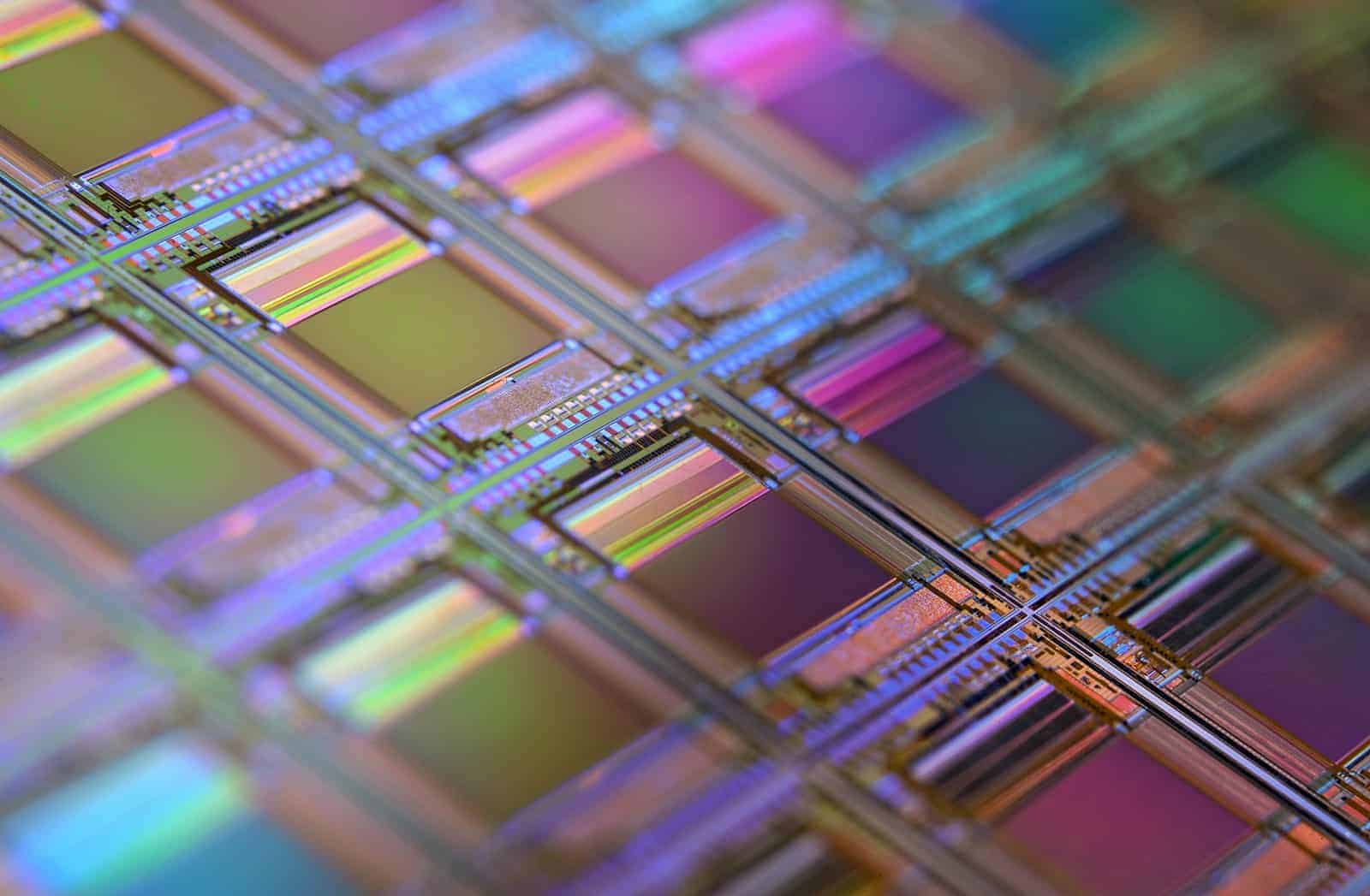
The 90nm chip process was a pivotal development in semiconductor manufacturing, marking a notable shrink in the size of integrated circuit features. When the semiconductor industry transitioned to this smaller, more efficient size around the years 2003 to 2005, it allowed for the creation of faster, more power-efficient chips. Companies like Intel were among the first to implement this advanced technology, paving the way for further miniaturization of electronic components.
Understanding the principles of this manufacturing process reveals why it represented such a significant evolution. By reducing the size of transistors to 90 nanometers, manufacturers could place more transistors on a chip, enhancing performance and reducing costs. This technology was not just about decreasing size; it also improved chip performance and facilitated the development of new applications across various sectors, including computing and telecommunications.
Key Aspects of the 90nm Chip Process
| Feature | Description | Companies Involved |
|---|---|---|
| Technical Definition | Refers to a semiconductor manufacturing process where the smallest feature size (e.g., transistor gate length) is approximately 90 nanometers. | Intel, AMD, IBM, TSMC, Fujitsu, Elpida, Texas Instruments, Micron Technology |
| Introduction | Became commercially available around 2003-2005. | – |
| Advantages over 130nm | * Smaller transistor sizes = more transistors per chip * Increased performance and/or reduced power consumption compared to the previous generation. | TSMC, Intel, AMD |
| Challenges | * Increased manufacturing complexity * Potential for defects and reliability issues at the smaller scale. | TSMC, Intel, AMD |
| Notable Chips (Examples) | * Intel Pentium 4, Celeron, Xeon * AMD Athlon 64, Sempron * IBM PowerPC G5 | Intel, AMD, IBM |
| Successor | 65nm process node | TSMC, Intel, AMD |
Important Notes
- “90nm” is a general term: Actual measurements might vary slightly between manufacturers.
- Rapid Evolution: Semiconductor manufacturing followed a fast pace of advancement; the 90nm node was quickly followed by 65nm, 45nm, and smaller processes.
- Legacy Technology: The 90nm process is now considered outdated, replaced by much smaller and more efficient fabrication processes.
Key Takeaways
- The 90nm process was a major advancement in chip miniaturization that occurred in the early 2000s.
- This manufacturing breakthrough allowed for improved chip performance and efficiency.
- Advancements in the 90nm technology facilitated new applications in various technology sectors.
Fundamentals of 90nm Semiconductor Manufacturing
The shift to the 90nm process in semiconductor manufacturing marked a significant step in the miniaturization of electronic components. This technology allowed for more powerful and energy-efficient devices.
Evolution from 65nm to 90nm Technology
The transition from the 65nm to the 90nm technology involved scaling up the silicon chip features to create more space for additional transistors. This change boosted the chip’s performance and reduced power consumption. Smaller process nodes meant a denser arrangement of transistors, directly influencing the chip’s computational capacity.
- 65nm technology: Aimed at increased transistor counts, smaller sizes
- 90nm technology: Enhanced performance, reduced power
Key Process Technologies in 90nm Fabrication
In 90nm fabrication, several key process technologies were prominent:
- Strained Silicon: Improves electron mobility, thus increasing performance.
- Low-k Dielectrics: Reduces capacitive delays, enhancing signal speed.
- Copper Interconnects: Offers better conductivity than traditional aluminum.
Each of these technologies contributed to the significant leaps in chip functionality seen in the 90nm era.
Lithography and Optical Proximity Correction
Lithography plays a pivotal role in etching the tiny, intricate patterns onto silicon wafers in the 90nm process. Advances in photolithography enabled manufacturers to meet the stringent design rules required at this scale. Optical proximity correction (OPC) was a critical technique used to adjust the masks in lithography to prevent errors due to light diffraction. This ensured that the printed patterns on silicon wafers accurately reflected the chip’s design.
90nm Chip Performance and Applications
The 90nm process marked significant strides in chip technology. This progression allowed for better performance and broadened the application range of integrated circuits.
Impact on Power Consumption and Management
Chips built using 90nm technology achieved notable improvements in power efficiency. The smaller size reduced the power needed for operations. Power management techniques became crucial at this node to optimize the battery life for mobile devices. Libraries tailored for 90nm processes included power-saving features like voltage islands and power gating, emphasizing the balance between power and performance.
Advancements in 90nm Integrated Circuits
The transition to 90nm process technology brought faster and more complex integrated circuits while reducing the area they required. This node allowed for denser layouts and enabled better performance thanks to its smaller features. It saw advancements in the construction of SRAM cells, achieving smaller and more efficient designs compared to its predecessors. The integration of low-k dielectric materials further propelled performance by reducing parasitic capacitance.
Application Spectrum: RF to Graphics Processing
Integrated circuits fabricated with 90nm technology found their place in a wide spectrum of applications, from RF components to complex graphics processing units. The size of chips for RF applications was critical, and the smaller footprint allowed them to fit into compact devices. On the other hand, graphics processors benefited from the increased speed and reduced power consumption, attributes essential for the demanding performance of video rendering.