Intel’s 18A process node is a cornerstone in the company’s strategy to reclaim leadership in semiconductor manufacturing. Slated for high-volume production in late 2025, 18A (short for “1.8nm-class”) introduces key technologies like RibbonFET (Intel’s gate-all-around transistor) and PowerVia, a backside power delivery system. These innovations promise dramatic gains in both performance and energy efficiency — and they’re just the beginning.
To address more specialized demands, Intel is building out a family of variants under the 18A umbrella: 18A-P, which enhances performance and efficiency, and 18A-PT, which brings advanced 3D stacking capabilities for next-generation AI and HPC workloads. Here’s how each node fits into Intel’s roadmap and the broader semiconductor landscape.
What Makes Intel 18A Unique?
The base 18A process node introduces two key features:
- RibbonFET: Intel’s first GAAFET (gate-all-around field-effect transistor), replacing FinFET for improved channel control and reduced leakage.
- PowerVia: A backside power delivery system that routes power through the bottom of the wafer, freeing the front side for better signal performance and reducing noise.
Compared to Intel 3, Intel claims that 18A provides:
- +25% performance at 1.1V
- –36% power at the same performance level
Intel 18A Variants Breakdown
| Variant | Key Focus | Notable Technologies | Production Timeline | Target Markets |
|---|---|---|---|---|
| 18A | General-purpose, scalable | RibbonFET, PowerVia | Risk in 2024, volume in H2 2025 | Client & server CPUs, foundry clients |
| 18A-P | Performance-optimized variant | Higher-performance transistor & power curves | 2026 | HPC, AI, networking, mobile SoCs |
| 18A-PT | Advanced 3D stacking | Foveros Direct, TSVs, <5μm hybrid bonding | ~2028 | AI accelerators, 3DIC, data center |
Intel 18A-P: The Performance-Centric Node
18A-P is a refinement of the base 18A process, tailored for customers who need even better power/frequency tradeoffs. This variant is part of Intel’s efforts to provide more customization within their process offerings — rather than a one-size-fits-all node.
- Designed for faster SoCs with tighter power budgets
- Wafers have already been produced, with first tape-outs by mid-2025
- Supported by expanded IP libraries from Cadence and Synopsys
Intel’s internal Panther Lake chips may incorporate elements of 18A-P, but its true value is expected to shine in AI and HPC markets, where every milliwatt counts.
Intel 18A-PT: The 3DIC Future
Intel 18A-PT builds on 18A-P and adds support for Foveros Direct, a next-gen 3D packaging technology enabling:
- <5µm pitch hybrid bonding
- Through-silicon vias (TSVs) for ultra-dense vertical integration
- Direct silicon-to-silicon stacking for heterogeneous computing
This positions 18A-PT as a key enabler for 3DIC architectures — something increasingly important in AI workloads, where compute and memory need to be tightly coupled.
Intel estimates that 18A-PT offers an 8% uplift in performance-per-watt over 18A-P in stacked designs — critical for power-constrained environments like edge AI or advanced mobile compute.
First Consumer Product: Panther Lake
- Panther Lake, Intel’s upcoming client CPU family, will be the first chip to roll out on 18A.
- Production begins in late 2025, with consumer PCs expected in early 2026.
- Panther Lake is expected to blend Lunar Lake’s power efficiency with Arrow Lake H’s performance, featuring updated Xe graphics and built-in AI acceleration.
Strategic Implications
Intel’s multi-node strategy with 18A, 18A-P, and 18A-PT is a direct response to competitive pressures from TSMC and Samsung — both of whom are accelerating their own GAAFET and 3D packaging roadmaps. While Intel has faced challenges securing external foundry customers (as confirmed by its CFO), major partnerships with Microsoft and interest from Nvidia and Broadcom signal growing momentum.
By expanding its foundry services portfolio with differentiated offerings like 18A-P and 18A-PT, Intel is moving beyond chasing process parity and toward providing custom-fit solutions for the increasingly fragmented chip market.
What’s Next?
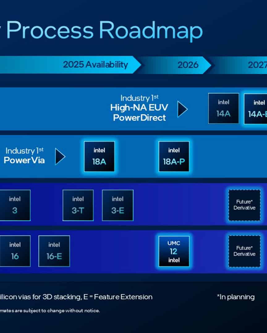
Looking ahead, Intel plans to follow 18A with 14A in 2027–2028, marking its transition to High-NA EUV lithography. Meanwhile, the success of 18A hinges not just on technical execution but on building a viable ecosystem of IP, tools, and customers — something Intel is aggressively courting via its IDM 2.0 strategy.
Whether Intel can truly rival TSMC at the foundry level remains to be seen, but with 18A and its variants, it’s clear that the company is no longer playing defense.
Key Takeaways
- Intel 18A technology comes in specialized variants with 18A-PT offering 8% better performance per watt for advanced computing needs.
- The 18A-PT variant specifically supports 3D integrated circuit designs through silicon via technology for improved communication.
- Intel’s expanding foundry roadmap demonstrates their strategy to create purpose-built manufacturing processes for different computing segments.
Overview of Intel 18A, Intel 18A-P, and Intel 18A-PT
Intel’s 18A technology represents a major leap in semiconductor manufacturing with innovative transistor designs and power delivery systems. The 18A family includes specialized variants tailored for different performance needs and applications.
Intel 18A Process Technology
Intel 18A introduces groundbreaking innovations that change how computer chips are made. At its core are two key technologies: RibbonFET transistors and PowerVia architecture. RibbonFET is Intel’s version of gate-all-around transistor technology, which improves control over current flow and reduces leakage.
PowerVia brings a revolutionary approach called backside power delivery. This moves power connections to the back of the chip, freeing up space on the front for more signal routing. The result is better power distribution and higher performance.
These technologies work together to increase transistor density while improving energy efficiency. Intel 18A represents Intel’s push to regain leadership in advanced chip manufacturing, competing directly with other industry leaders.
Intel 18A-P and Intel 18A-PT Innovations
Intel 18A-P is a specialized variant of the base 18A technology. It’s designed to deliver enhanced performance for a broader range of customers. This version features an optimized power and frequency curve that provides an 8% improvement in performance per watt compared to standard 18A.
Intel 18A-PT takes things even further. It builds upon the 18A-P advancements but is specifically designed for AI and high-performance computing (HPC) applications. 18A-PT is particularly valuable for next-generation 3DIC (three-dimensional integrated circuit) designs.
The “-PT” variant leverages the performance and power efficiency gains of 18A-P while adding connectivity features that benefit complex computing systems. Early wafers have already been produced, showing Intel’s commitment to bringing these technologies to market.
Performance and Energy Efficiency
The Intel 18A family delivers significant gains in both performance and energy efficiency. The base 18A technology improves on previous generations through its RibbonFET transistors and PowerVia architecture, reducing power consumption while increasing processing capability.
Intel 18A-P takes this further with its optimized power/frequency curve. The 8% improvement in performance per watt means systems can do more work using the same amount of energy, or maintain performance while using less power.
For demanding AI and HPC workloads, Intel 18A-PT provides the highest performance profile. It manages inductive power droop (sudden voltage drops) more effectively, maintaining stable operation under heavy loads.
All three variants share the fundamental improvements in iso-power performance (speed at the same power level) while offering different optimization points for various applications and customer needs.
Manufacturing, Ecosystem, and Industry Impact
Intel’s 18A technology nodes represent a significant leap in semiconductor manufacturing, supported by robust partnerships and supply chain innovations. These advancements are reshaping how chips are designed, produced, and integrated into emerging applications across various industries.
Intel Foundry and Advanced Manufacturing
Intel 18A has reached risk production status and is expected to move into volume manufacturing in 2025. This marks a crucial milestone in Intel’s manufacturing roadmap and its competitive position in the advanced node market. The company has invested heavily in U.S. manufacturing facilities to support these cutting-edge processes.
Intel’s fabrication capabilities for 18A include specialized variants like 18A-P and 18A-PT, each designed for specific performance requirements and applications. The 18A-PT variant specifically supports Foveros Direct 3D technology with hybrid bonding interconnects.
Manufacturing of these advanced nodes requires extreme precision and new tooling systems. Intel has worked to refine these processes through extensive test chip production and validation cycles before moving to full production.
Ecosystem Partnerships and Supply Chain
Intel has built a comprehensive foundry ecosystem to support 18A production. This includes partnerships with materials suppliers, equipment manufacturers, and testing services that ensure a robust supply chain.
The company has established several chiplet alliances to standardize interfaces and promote interoperability between different chip components. These collaborations help address semiconductor supply chain challenges that have affected the industry in recent years.
Intel Foundry Portal serves as a central hub for partners and customers to access resources, submit designs, and track production status. The Direct Connect Conference and Intel Foundry Conference have become key events for ecosystem alignment.
Intel’s engineering-first culture drives continuous improvement in manufacturing processes and supply chain resilience. This approach helps maintain quality while advancing node technology.
EDA, IP, and Design Enablement
Intel works closely with major Electronic Design Automation (EDA) providers including Cadence, Siemens, and Synopsys to create tools that support 18A designs. These partnerships ensure that chip designers have the software needed to utilize Intel’s advanced processes.
Process Design Kits (PDKs) for Intel 18A and its variants provide designers with the technical specifications needed to create compatible chips. These kits include detailed documentation, validation rules, and simulation models.
The company offers a range of intellectual property (IP) blocks optimized for 18A, allowing faster time-to-market for customers. Reference flows demonstrate best practices for design implementation.
The Intel Foundry Accelerator Ecosystem helps smaller companies and startups access design services and tools needed for 18A adoption. This program has expanded the potential user base for Intel’s advanced nodes.
Emerging Applications and Market Influence
Intel 18A technologies are poised to power next-generation cloud infrastructure, generative AI systems, and high-performance computing applications. The performance and efficiency gains enable new capabilities in these demanding workloads.
Panther Lake processors and Clearwater Forest server processors are among the first products expected to utilize 18A technology. These chips will showcase the benefits of advanced node manufacturing.
High-bandwidth memory integration is a key focus area for 18A-PT with its advanced packaging capabilities. This addresses the growing need for faster memory access in AI and data-intensive workloads.
The broader semiconductor industry is watching Intel’s 18A execution closely, as success could shift competitive dynamics and influence future technology roadmaps. Many companies are already designing products that will take advantage of these manufacturing advances when they reach full production.
Frequently Asked Questions
Intel’s 18A process technology comes with several variants designed for different performance needs. These new manufacturing processes represent significant advancements in semiconductor technology with specific benefits for AI and high-performance computing applications.
What distinguishes the Intel 18A-P and Intel 18A-PT variants in terms of performance?
Intel 18A-P is a high-performance variant of the base 18A node. It offers approximately 8% better performance per watt compared to the standard 18A process. Early wafers of 18A-P are already running through Intel’s fabrication facilities.
Intel 18A-PT builds upon the 18A-P, leveraging its performance and power efficiency gains. This variant is specifically designed for AI and high-performance computing customers who are developing next-generation 3DIC (three-dimensional integrated circuit) designs.
How does Intel’s 18A process technology compare with TSMC’s 2nm process?
Intel 18A is positioned to compete directly with TSMC’s 2nm manufacturing process. Both technologies represent the cutting edge of semiconductor fabrication, with similar transistor densities and power efficiency targets.
Intel claims its 18A process will offer competitive performance advantages, though real-world comparisons will only be possible once both technologies reach volume production. The competitive landscape between these two processes will likely shape the high-performance computing market for years to come.
What is the expected yield rate for Intel’s 18A manufacturing process?
Specific yield rates for Intel’s 18A process have not been publicly disclosed. As with any new semiconductor process, yields typically start lower during early production and improve over time as manufacturing processes mature.
Industry analysts expect initial yields to follow standard patterns for leading-edge nodes, with gradual improvements as Intel refines the manufacturing process. Yield rates will be crucial for determining the commercial viability and cost-effectiveness of chips made using this process.
Where are Intel’s 18A manufacturing facilities located?
Intel is producing 18A chips at its leading-edge fabrication facilities in the United States. Key manufacturing sites include facilities in Arizona, Oregon, and New Mexico.
The company has made significant investments in expanding its manufacturing capabilities as part of its IDM 2.0 strategy. These facilities are equipped with the advanced equipment needed for the specialized manufacturing steps required by the 18A process.
When is the Intel 18A process node expected to be released?
Intel 18A is scheduled for release in the second half of 2025. The company has indicated that development is progressing as planned, with early 18A-P wafers already running through production.
This timeline puts Intel in a competitive position against other semiconductor manufacturers’ advanced nodes. The company has been working to accelerate its process technology roadmap after previous delays with earlier nodes.
What are the implications of Intel’s 18A process node for high-performance computing and gaming?
The 18A process will enable more powerful and energy-efficient processors for high-performance computing and gaming applications. Its advanced transistor architecture should provide significant performance gains while reducing power consumption.
For gaming, this could translate to higher frame rates and more detailed graphics in future processors. In high-performance computing, the efficiency improvements offered by 18A will be particularly valuable for data centers and AI applications, potentially reducing operating costs while increasing computational capabilities.