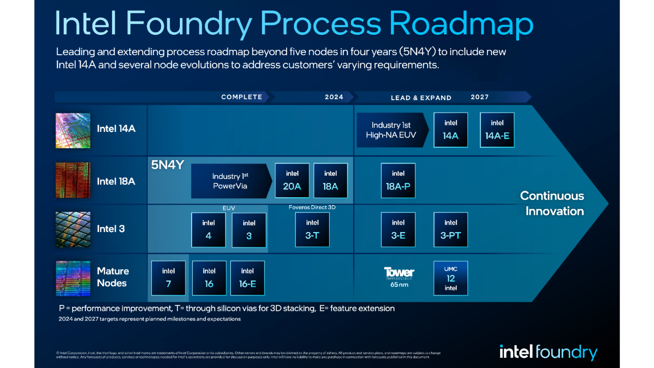
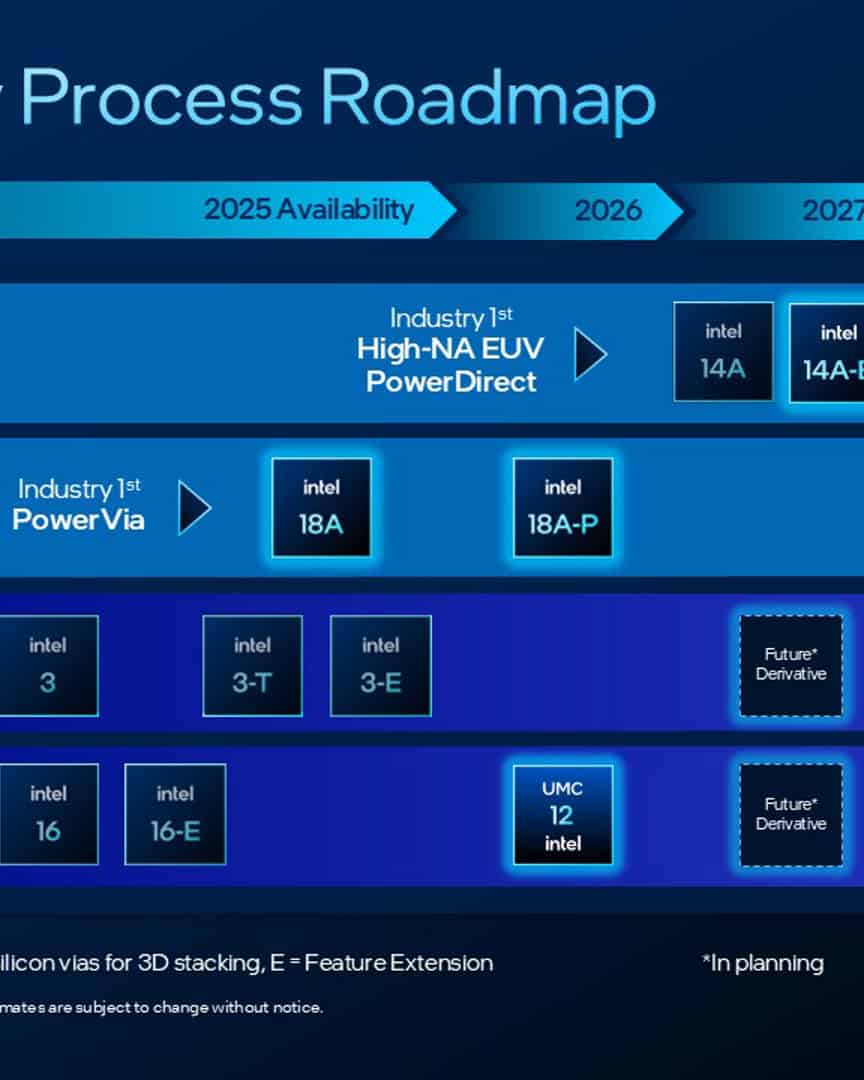
Intel’s upcoming 14A process node isn’t just another incremental step forward—it’s a bold leap into the angstrom era of chip manufacturing. Positioned to enter risk production in 2027 and mass production in 2028, 14A (short for 1.4nm-class) introduces several industry-first innovations that could redefine performance benchmarks for CPUs, GPUs, and AI accelerators.

Breaking Ground With High-NA EUV
The crown jewel of 14A is its adoption of High-NA EUV lithography, a revolutionary advancement in chip patterning technology. Unlike today’s extreme ultraviolet (EUV) systems, High-NA (Numerical Aperture) EUV allows for much finer feature definition, enabling higher transistor density and better performance scaling.
Intel will be the first company to commercialize High-NA EUV, giving it a potential multi-year head start over rivals like TSMC and Samsung. TSMC’s competing 1.4nm-class node isn’t expected until at least 2028—and notably, it won’t use High-NA EUV at launch.
PowerDirect: A Smarter Way To Deliver Power
Building on the PowerVia backside power delivery system introduced in Intel’s 18A node, 14A debuts the more advanced PowerDirect architecture. This second-gen power delivery approach feeds power directly to the source and drain of each transistor, minimizing resistance and reducing power waste. The result? Lower energy consumption and better thermal efficiency—key for both data centers and portable devices.
Turbo Cells: Speed Meets Efficiency
Intel is also introducing a new standard cell architecture called Turbo Cells, designed specifically to maximize frequency scaling while reducing switching power. These cells are aimed at high-performance computing and AI workloads, offering a power-efficient route to higher clock speeds and computational throughput. They represent another weapon in Intel’s toolkit for competing with the growing dominance of ARM-based designs.

Projected Performance Gains
Intel estimates the 14A node will deliver:
- 15–20% higher performance over 18A
- 25–35% lower power consumption
- Improved logic density, which reduces die size and manufacturing cost per transistor
These gains are particularly significant in AI, where power efficiency and computational throughput are critical bottlenecks for large-scale inference and training.
Customer Pipeline & Production Plans
Risk production is scheduled for 2027, with mass production starting in 2028. Intel has already distributed early Process Design Kits (PDKs) to strategic partners and lead customers, allowing them to begin test chip development.
However, uptake from external foundry clients remains modest. Intel CFO David Zinsner recently noted that customer commitments are limited at this stage, though this is not unusual for a node that’s still two years from risk production. Intel aims to increase adoption to help its foundry division reach breakeven by 2027.
The Bigger Picture: Intel’s Foundry Comeback
Intel 14A is a critical part of the company’s broader effort to regain semiconductor leadership and re-establish Intel Foundry as a competitive alternative to TSMC and Samsung. Alongside 14A, Intel has also introduced:
- 18A (1.8nm): Currently in production for both internal products and external foundry customers
- 14A-E: A variant of 14A, optimized for extended features and expected to be ready in parallel with the standard node
If successful, 14A could restore Intel’s standing as a process technology leader—an area where it lost ground over the past decade due to delayed transitions and manufacturing challenges.
What This Means for AI, Mobile, and HPC
With improved power efficiency, smaller form factors, and higher frequencies, 14A is tailor-made for emerging markets like:
- AI accelerators – especially where thermal limits constrain scaling
- High-performance CPUs and GPUs – targeting both server and enthusiast platforms
- Next-gen mobile SoCs – potentially competing with ARM-based designs in laptops and handhelds
Final Outlook
Intel’s 14A node could mark a turning point not just for Intel, but for the entire semiconductor industry. With High-NA EUV, PowerDirect, and Turbo Cells, it introduces foundational innovations that extend beyond marketing buzzwords and into measurable benefits. But execution will be key. If Intel can deliver on its promises, 14A may be the tech cornerstone that powers the next wave of AI, cloud, and computing experiences by the end of the decade.
Key Takeaways
- Intel 14A will deliver 15-20% better performance-per-watt with new “turbo cell” technology that boosts CPU speeds.
- The new process node follows Intel’s 18A technology and is expected to begin risk production in 2027.
- Intel is using a strategic mix of manufacturing technologies, including limited High-NA EUV implementation for specific chip layers.
Overview of Intel 14A Technology
Intel is working on a new chip process called 14A that promises big improvements for future processors. This next-generation technology will follow Intel’s 18A node and is expected to deliver 15-20% better performance-per-watt compared to previous designs. Intel’s 14A process introduces innovative “turbo cell” technology designed to boost CPU speeds and maximum frequencies, giving computers extra power when needed.
One of the most exciting features of 14A is this new “turbo cell” approach. It aims to push processors to run faster while still being energy efficient. Intel is also implementing a second-generation technology called PowerDirect with 14A, which further improves how the chips use energy. The company is already working with lead customers on 14A designs, with risk production planned for 2027.
Intel plans to use advanced High-NA EUV manufacturing technology for some layers of the 14A chips. This selective approach shows Intel’s careful strategy in adopting new manufacturing methods. By combining several new technologies, Intel hopes to stay competitive in the chip manufacturing race against rivals.
Intel 14A represents the next major advancement in Intel’s semiconductor manufacturing process. This technology promises significant performance and efficiency improvements through innovative design techniques, specialized cells, and new lithography methods.
Position in Intel’s Process Roadmap
Intel 14A follows the Intel 18A node in the company’s foundry roadmap. It marks an important step in Intel’s manufacturing strategy as the company works to regain leadership in semiconductor production. Intel has positioned 14A as part of its “Systems Foundry” approach, which focuses on creating specialized manufacturing processes for the AI era.
The numbering might seem confusing since 14 is smaller than 18, but in Intel’s naming convention, smaller numbers traditionally indicated more advanced nodes. Intel 14A builds upon technologies introduced in earlier nodes including Intel 4, Intel 16, and Intel 18A.
Intel has featured 14A prominently in its recent foundry announcements, signaling the company’s confidence in this manufacturing process to deliver competitive advantages against rivals like TSMC and Samsung.
Intel 14A vs Intel 18A and Previous Nodes
Intel 14A offers substantial improvements over its predecessor, Intel 18A. According to Intel’s disclosures, 14A delivers a 15-20% increase in performance-per-watt compared to 18A. This improvement can be leveraged in two ways: either higher clock speeds for better performance or 25-35% lower power consumption at the same performance level.
The node also represents approximately a 1.3x improvement in density compared to previous technologies. This means more transistors can fit in the same area, enabling more complex chips.
Intel’s process evolution from earlier nodes like Intel 4 and Intel 16 to 18A and now 14A shows the company’s commitment to advancing its manufacturing capabilities. Each node has built upon previous technologies while introducing new innovations to improve performance and efficiency.
Key Innovations in 14A Process Technology
Intel 14A introduces several breakthrough technologies. One major innovation is “Turbo Cells,” which help unlock higher performance levels. These specialized cells allow for more efficient power delivery and management across the chip.
Another key advancement is PowerDirect, a second-generation implementation that significantly boosts energy efficiency. This technology helps manage power consumption more effectively, contributing to the overall performance-per-watt improvements.
Perhaps most notably, Intel 14A employs directed self-assembly (DSA) for lithography. This technique has been described as Intel’s “magic bullet” for dramatically lowering manufacturing costs. DSA allows for more precise pattern creation without requiring the most expensive extreme ultraviolet (EUV) lithography tools for every layer.
These innovations collectively enable Intel 14A to deliver meaningful improvements for next-generation computing needs, especially for AI and high-performance applications.
Technical Advancements and Industry Impact
Intel’s 14A process represents significant technological innovation in semiconductor manufacturing, combining several cutting-edge techniques that promise to reshape chip production. The advancements focus on improving power efficiency, performance, and manufacturing capabilities to meet the demands of AI and other compute-intensive applications.
RibbonFET and PowerVia Enhancements
Intel’s 14A builds upon the foundation laid by its 18A node, further refining the RibbonFET architecture. RibbonFET represents Intel’s implementation of Gate-All-Around (GAA) transistor design, which improves electrical flow control compared to FinFET technology.
The 14A node introduces PowerDirect, an enhanced version of the PowerVia backside power delivery system. This technology routes power through the back of the silicon wafer, allowing signal routing to occupy the entire front side.
This separation reduces interference and power delivery issues in complex chip designs. PowerDirect in 14A appears to deliver even better results than the original PowerVia implementation, with reports indicating yield improvements of 28% in Q1 2025.
Manufacturing data suggests these enhancements contribute to a planned 40% capacity boost for Intel’s production lines.
High-NA EUV Lithography and Patterning Technology
Intel’s 14A process employs advanced lithography techniques, with the company pursuing dual strategies. While preparing for High-NA (Numerical Aperture) EUV implementation, Intel has developed alternative Low-NA techniques that reportedly achieve identical yield and design rules.
This hedged approach provides manufacturing flexibility while the more expensive High-NA EUV equipment matures. The patterning technology enables smaller feature sizes and more precise circuit layouts.
Intel’s 14A lithography improvements support:
- Finer circuit patterns
- Higher transistor density
- Better manufacturing precision
- Reduced defect rates
This multi-pronged approach to lithography helps Intel manage both technological and economic risks in advanced chip manufacturing.
Power Efficiency and Performance Per Watt
The 14A node delivers remarkable power efficiency gains, with reports indicating up to 35% less power consumption than its predecessor, the 18A node. This improvement stems from:
- More efficient transistor designs
- Reduced electrical resistance
- Better heat management
- Optimized power delivery
These enhancements directly translate to better performance per watt, making 14A-based chips ideal for applications where energy efficiency is critical. Data centers, mobile devices, and embedded systems particularly benefit from these improvements.
The reduced power requirements also help address thermal constraints that often limit sustained performance in modern processors.
Applications in the AI Era and Chip Design
Intel positions 14A as the foundation of its “Systems Foundry” approach, specifically designed for AI-era computing needs. The process technology enables chips that can handle the intense computational workloads of machine learning while maintaining reasonable power budgets.
The 14A node supports specialized chip designs beyond traditional CPUs, including:
- Neural processing units
- AI accelerators
- High-bandwidth memory interfaces
- Mixed-signal components
Intel’s roadmap places 14A as entering volume production from 2027 onward. The technology represents Intel’s bid to regain manufacturing leadership in the foundry space, particularly for advanced AI and computing applications.
The improved manufacturing yields and planned capacity increases suggest Intel is preparing for significant customer demand for 14A-based chips.
Frequently Asked Questions
Intel’s 14A process node represents a significant advancement in semiconductor technology. This new manufacturing technology introduces several key innovations and continues Intel’s path toward regaining leadership in chip fabrication.
When is the expected release date for the Intel 14A node?
Intel has scheduled the 14A node for production in the second half of 2026. The company has been working to keep this timeline despite industry challenges in advanced manufacturing processes.
The foundry roadmap now shows 14A-E as part of the standard offering rather than the original 14A. This suggests some modifications to the initial release plans.
What are the specifications of the Intel 14A technology?
The 14A node will use a combination of traditional EUV and High-NA EUV lithography. Intel plans to implement High-NA EUV for a limited number of critical layers in the manufacturing process.
A key innovation in 14A is directed self-assembly (DSA) technology. This approach helps reduce manufacturing costs while maintaining advanced performance characteristics.
How does the cost of Intel 14A compare to previous generations?
The implementation of directed self-assembly significantly lowers lithography costs compared to previous nodes. This is particularly important as chip manufacturing costs have risen dramatically with each new generation.
The selective use of expensive High-NA EUV lithography only for critical layers helps control costs while maintaining performance advantages.
What advancements does Intel 14A offer over its predecessors?
The 14A node offers improved transistor density and power efficiency over previous generations. These improvements will enable more powerful and energy-efficient chips.
The introduction of directed self-assembly represents a major technical breakthrough that could give Intel an advantage in manufacturing economics.
Has Intel transitioned to a 7nm process technology with its recent nodes?
Intel has moved beyond the traditional nanometer naming convention with its recent nodes. Rather than using the “7nm” label, Intel has adopted a new naming system with nodes like 20A and 14A.
The “A” refers to angstroms (Å), with one angstrom equaling 0.1 nanometers. This puts the 14A roughly equivalent to what other manufacturers might call a 1.4nm process.
What is the current status of the Intel 20A node development?
Intel’s 20A node is currently in development and scheduled to precede the 14A node. It introduces key technologies like RibbonFET transistors and PowerVia backside power delivery.
The progress of 20A is critical as it establishes the foundation for many technologies that will carry forward to the 14A node.