The semiconductor industry is changing significantly, with more focus on making chips in the U.S. This shift comes from worries about supply chain problems, national security, and keeping the economy competitive. The U.S. government has acted by passing the CHIPS and Science Act, which gives billions of dollars to support domestic chip manufacturing. This law has encouraged major investments from global chipmakers, especially TSMC, the largest contract chip maker in the world. TSMC’s multi-billion dollar investment in Arizona is a big step for the U.S. semiconductor industry and could lead to a rebirth of American chip production.
This effort aims to build not just factories, but an entire ecosystem, including research and development, manufacturing, and supply chains, all within the U.S. The push for more semiconductor manufacturing in the U.S. has led to large investments in projects like TSMC’s new facility in Phoenix, Arizona, raising questions about government spending. While TSMC’s facility shows the potential benefits of strategic government support, it also creates challenges that need to be solved for successful and lasting growth in U.S. semiconductor manufacturing.
TSMC’s Arizona Fab: A New Era for U.S. Chipmaking
The Push for Domestic Chip Production
The global chip shortage showed how important it is for the U.S. to make its own advanced semiconductors. TSMC, the world’s largest contract chipmaker, is building a major manufacturing plant in Phoenix, Arizona. This project aims to bring cutting-edge chip production back to American soil. The first fab is slated to begin production in early 2025 using the N4 process. This is a big deal for the U.S. tech industry.
What is the N4 Process?
TSMC’s N4 process is a refined version of its 5nm technology. It offers better performance and power efficiency than previous generations. This technology is used to make chips for many devices, including smartphones, high-performance computing, and AI applications. This is not the most leading-edge technology TSMC offers, but it is still very advanced and will be used in many products.
The Arizona Timeline and Expansion
TSMC’s Arizona project has grown significantly. Here’s a breakdown:
- 2020: Initial announcement of a $12 billion investment for one fab.
- 2022: Announcement of a second fab using 3nm technology.
- April 2024: Announcement of a third fab using 2nm or more advanced technology, with production starting by the end of the decade, and securing $6.6 billion in CHIPS Act funding.
The first fab is expected to start producing chips in early 2025. The second fab is planned for 2028, and the third fab is expected to start production by the end of the decade. The total investment is now over $65 billion. This shows TSMC’s long-term commitment to U.S. manufacturing.
The CHIPS Act and its Impact
The CHIPS and Science Act is a U.S. government initiative to boost domestic semiconductor production. TSMC is set to receive up to $6.6 billion in direct funding from this Act. This funding is critical for offsetting the higher costs of building and operating fabs in the U.S. compared to other regions. It is also a key factor in TSMC’s decision to expand its Arizona operations.
Jobs and Economic Benefits
The TSMC Arizona facility is expected to create thousands of high-paying jobs in the region. It will also support other businesses in the supply chain, creating even more economic opportunities. This project is a major boost for the Arizona economy and the U.S. economy as a whole. A mixed use development called Halo Vista is also being built to support the influx of employees and their families. This $7 billion development will include nearly 9,000 housing units.
Comparing TSMC’s Arizona Fabs
| Fab | Process Technology | Expected Production Start |
|---|---|---|
| Fab 1 | N4 | Early 2025 |
| Fab 2 | N3 | 2028 |
| Fab 3 | 2nm or more advanced | End of the decade |
Potential Challenges
Building and operating advanced chip fabs in the U.S. is not without challenges. These include:
- Higher Costs: Building and operating fabs in the U.S. is generally more expensive than in Asia.
- Skilled Labor Shortage: Finding enough skilled workers to operate these complex facilities could be a problem.
- Supply Chain Issues: Establishing a robust domestic supply chain for chip manufacturing will take time and effort.
The Bigger Picture: U.S. Semiconductor Independence
TSMC’s Arizona project is part of a larger effort to make the U.S. more self-sufficient in semiconductor manufacturing. This is important for national security and economic competitiveness. By bringing chip production back to the U.S., the country can reduce its reliance on foreign suppliers and protect itself from future supply chain disruptions. Other companies like Intel and GlobalFoundries are also expanding their U.S. manufacturing. This signals a turning point for the U.S. semiconductor industry.
The push for domestic chip manufacturing extends beyond just securing supply chains; it’s also about fostering innovation and technological leadership. By investing in advanced manufacturing within the U.S., the nation aims to reclaim its position at the forefront of semiconductor technology. This not only bolsters economic growth but also strengthens national security by reducing reliance on potentially unstable or adversarial sources for critical technologies. The impact of these investments will ripple through various sectors, from consumer electronics to defense systems, solidifying the U.S.’s position in the global tech landscape. These investments are designed to create a positive feedback loop, where domestic production fuels further research and development, ensuring that the U.S. remains at the cutting edge of semiconductor innovation for years to come.
Short Summary:
- The CHIPS and Science Act allocates substantial funds to promote domestic semiconductor manufacturing.
- TSMC is set to invest over $65 billion in its Phoenix facility, including significant federal funding.
- While TSMC’s expansion promises economic growth and job creation, it faces challenges adapting its corporate culture to the U.S. workforce.
Recent developments are aimed at boosting the semiconductor industry in the United States, with a strong emphasis on domestic manufacturing to decrease reliance on foreign supply chains. The CHIPS and Science Act, signed into law in August 2022, allocates $52.7 billion for semiconductor manufacturing and research initiatives. This marks a significant shift in the U.S. government’s approach to supporting this critical sector.
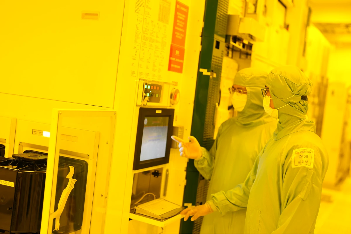
One notable example of this effort is in Arizona, where the Taiwan Semiconductor Manufacturing Company (TSMC) plans to build a state-of-the-art fabrication plant. TSMC’s new facility highlights the implications of the CHIPS Act, as the company intends to invest more than $65 billion in total, with the U.S. Department of Commerce committing up to $6.6 billion in direct funding to support this development. During a recent site inspection with Marketplace’s Kai Ryssdal, Heather Long, a columnist for the Washington Post, remarked, “This is ground zero for the new economy… They’re about to get an even bigger infusion of cash from the federal government.”
The region, referred to as the “Silicon Desert,” aims to establish Arizona as a hub for semiconductor innovation, ultimately creating thousands of jobs. Historically, Phoenix has been involved in the semiconductor market, with companies like Motorola and Intel having a presence in the area. However, the funding from the CHIPS Act creates opportunities for unprecedented growth.
Intel received $8.5 billion in direct funding and plans to invest an additional $20 billion in new facilities. Meanwhile, TSMC is working on expanding its operations with three fabrication plants, with an estimated total cost exceeding $65 billion. As TSMC moves forward with the completion of its first plant and begins work on the second, the company has recently announced plans for a third facility to better meet customer demands. TSMC Chairman Dr. Mark Liu has acknowledged this historic investment, stating,
“The CHIPS and Science Act provides TSMC the opportunity to make this unprecedented investment and to offer our foundry service of the most advanced manufacturing technologies in the United States.”
This statement echoes the government’s ambition to fortify national security while also enhancing the U.S. semiconductor ecosystem.
The economic impact of TSMC’s operations cannot be understated. With each of the three planned fabs expected to create approximately 6,000 direct jobs, the ramifications of this investment include not only direct employment but also estimated indirect job creation that could total tens of thousands across the region. According to the Greater Phoenix Economic Council, TSMC’s efforts stand to generate more than 20,000 unique construction jobs, ensuring a ripple effect throughout the local economy.
TSMC further outlines a commitment to using cutting-edge technology in its cleanroom areas, designed to be significantly larger than industry standards to accommodate high-tech manufacturing. Their operations are expected to leverage advanced 4nm and 2nm process technologies. Production for chips using the 4nm process is slated to begin in the first half of 2025, while the second fab is expected to produce the next-generation 2nm technology by 2028. The rapid development underscores the speed with which TSMC intends to set up operations compared to the old, slow supply chains characterized by predominately overseas reliance.
Environmental considerations are woven into TSMC’s plans. The company has adopted green manufacturing practices and targets achieving a 90% water recycling rate at its facilities. TSMC has begun efforts to construct a water reclamation plant designed to implement a “near zero liquid discharge” system aimed at reducing ecological impact.
In addition to financial commitments, TSMC’s partnership with the federal government comes alongside potential loans of up to $5 billion and various tax credits designed to ensure the competitiveness of their venture in a financially sustainable way. However, these moves are not without skepticism. Observers question whether the U.S. industrial and regulatory environment can accommodate TSMC’s ambitious goals, especially considering the differences in work culture between Taiwan and the U.S.
Managing workers from both regions poses a significant challenge. As noted by Dr. C.C. Wei, TSMC’s CEO, his company’s success is deeply tied to the innovation and effort of the workforce:
“We are honored to support our customers who have been pioneers in mobile, artificial intelligence, and high-performance computing. As their foundry partner, we will help them unleash their innovations.”
However, cultural discrepancies and challenges in communication have become apparent as American and Taiwanese engineers work together.
Reported findings from former employees depict a tense atmosphere in which many American engineers have struggled to adapt to the company’s rigorous work environment, which is characterized by long hours and a strict hierarchical command structure. Bruce, a U.S. engineer, voiced his concerns over the discrepancies between expectations of the Taiwanese framework and those prevalent among American colleagues. He stated he initially realized the high level of rigor imparted by the company was overwhelming, leading him to question his decision to join.
With around 2,200 employees currently operating at TSMC Arizona, a significant portion of which hail from Taiwan, there are ongoing tensions regarding the integration of American and Taiwanese work ethics and expectations. Many American engineers have voiced frustrations about the rigidity of TSMC’s operational approach and noted that the exigencies of Taiwanese workers contrast with their own work-life balance desires. As one engineer described,
“The Taiwanese create this false sense of urgency with every single task…”
This model promotes a level of intensity that many American employees find alien and exhausting.
As TSMC insists upon moving forward, they face the challenge of adapting their operations to ensure they are competitive within the U.S. labor framework, which includes negotiating labor laws, managing expectations of their highly skilled workforce, and securing a smooth workflow conducive to innovation. While the facility promises progress on domestic semiconductor manufacturing, the ultimate success of TSMC’s venture in Phoenix will depend as much on the company’s ability to foster a collaborative environment as on its financial investments.
As the years unfold, TSMC’s Phoenix site is positioned to play a pivotal role in realizing these ambitions. Whether it will become a model of successful cooperation between distinct cultural working styles remains to be seen.
The excitement and anticipation surrounding TSMC’s investment highlight a critical moment for the American semiconductor landscape. Yet, the intricacies of this ambitious project emphasize the broader implications of government spending in fostering sustainable and strategic industry growth.